High-Density Grinding Media Balls for Industrial Applications

Semiconductor Grade Silicon Carbide Powder: The Core of Your Research
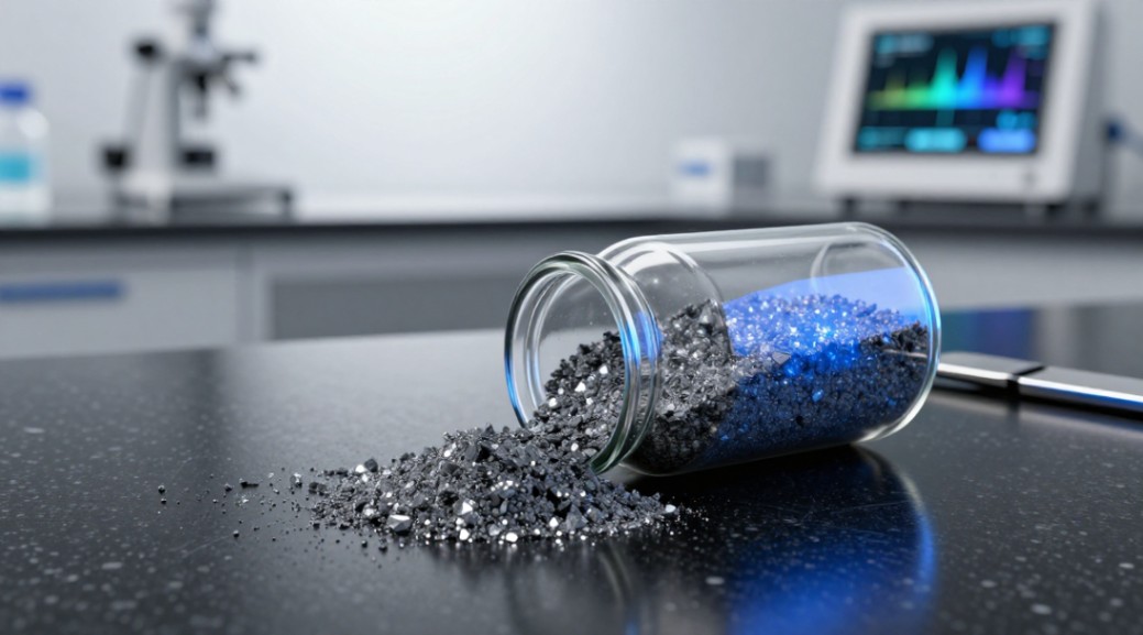
In advanced semiconductor research, your starting material dictates your project’s ceiling. For wide-bandgap work, semiconductor grade silicon carbide powder isn’t just a commodity; it’s the foundational element. Think of it as the single-crystal silicon of the high-power, high-temperature future. Most labs waste months debugging processes that trace back to inconsistent powder quality. The central conflict isn’t about finding powder-it’s about identifying the specific grade that aligns with your exact application, whether that’s bulk crystal growth, thin-film deposition, or additive manufacturing of ceramic components.
Critical Properties and the Research Implications
This powder’s utility stems from extreme physical properties. Its wide bandgap enables devices that operate at voltages and temperatures impossible for silicon. The high thermal conductivity is non-negotiable for power electronics, pulling heat away from critical junctions. Chemical inertness and supreme hardness make it ideal for advanced ceramics facing corrosive or abrasive environments. However, these macroscopic properties are useless if the powder’s micro-scale characteristics-purity, polytype, and morphology-aren’t rigorously controlled. Your device performance is hostage to your powder’s pedigree.
The Defining Comparison: 4H-SiC vs. 6H-SiC Polytypes
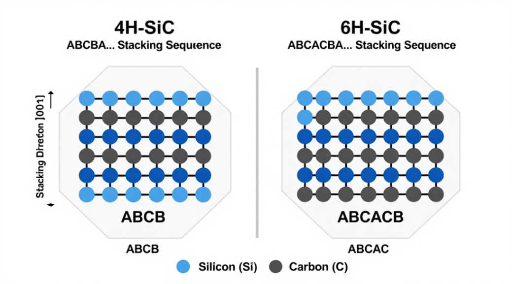
Choosing the wrong polytype is a fatal, irreversible error for electronic device research. The industry standard narrative often oversimplifies. This table cuts through the noise.
Polytype Comparison for Semiconductor Research
| Parameter | 4H-SiC (The Modern Standard) | 6H-SiC (The Legacy Workhorse) |
|---|---|---|
| Crystal Structure & Bandgap | Hexagonal, ~3.26 eV. Wider, more isotropic. | Hexagonal, ~3.02 eV. Slightly narrower. |
| Electron Mobility | Higher (~950 cm²/V·s). Superior for high-frequency MOSFETs and RF devices. | Lower (~450 cm²/V·s). Acceptable for some diodes and optoelectronics. |
| Primary Research Application | Cutting-edge vertical power devices (MOSFETs, IGBTs), RF electronics. The future-forward choice. | LED substrates (historically), some high-temperature sensors, foundational crystal growth studies. |
| Key Advantage | Best-in-class electronic performance for modern power and RF systems. Dominates commercial device roadmaps. | Often more readily available in bulk, lower cost for non-critical electronic or mechanical studies. |
| Fatal Flaw for Researchers | Demands extreme purity and stoichiometry. Contamination or stacking faults ruin device yield. | Inferior electron mobility limits performance ceiling for advanced power switching applications. |
| Our Verdict | Mandatory for any research targeting state-of-the-art electronic devices. Don’t compromise here. | Only select for historical comparison studies, specific optoelectronic work, or purely mechanical ceramic applications. |
Beyond Polytype: The Make-or-Break Specifications
Polytype is just the first filter. Real research-grade material is defined by specs that separate lab-ready powder from industrial abrasive. The purity requirement starts at 99.9995% (5N5) and goes higher. Trace metallic impurities-Al, Fe, Ti, V-act as deep-level traps, killing carrier lifetime. Particle size distribution (PSD) must be tight. A broad PSD leads to inconsistent packing, sintering, and vapor transport. Morphology matters: angular, fractured particles behave differently in a CVD crucible than smooth, spherical ones from laser pyrolysis. Crystallinity must be single-phase. Amorphous or secondary polytype inclusions create defects that propagate into your final crystal or coating.
Synthesis Methods: Understanding Your Powder’s Origin Story
How the powder is made determines its innate characteristics. You cannot separate synthesis from suitability.
- Acheson Process (Carbothermal Reduction): The old guard. Produces large volumes of powder, often with a mix of polytypes and higher impurity levels. It’s cost-effective for bulk ceramic applications but a gamble for advanced semiconductor work unless extensively purified and classified. Assume it needs post-processing.
- Chemical Vapor Deposition (CVD): The high-purity champion. CVD-derived powder typically offers the best stoichiometry, highest purity, and controlled polytype formation (like 4H-SiC). It’s the preferred source for serious crystal growth research. The trade-off is cost and often smaller batch sizes.
- Laser Pyrolysis (Vapor Phase Synthesis): The morphology specialist. Excels at producing ultra-fine, spherical, and highly uniform nanoparticles. Invaluable for research into nano-composites, specialized coatings, or where surface area is critical. Purity can be high, but scalability for bulk crystal growth is limited.
Procurement Table: Decoding Supplier Specifications for Research
Comparing supplier datasheets is frustrating. They highlight different metrics. This framework standardizes the comparison to focus on what impacts research outcomes.
Research Procurement Evaluation Matrix
| Evaluation Criteria | What to Look For (The Good) | Red Flags (Walk Away) |
|---|---|---|
| Purity & Impurity Analysis | Detailed GDMS or ICP-MS report showing total metallic impurities <10 ppm, with specific callouts for critical killers like Vanadium <0.5 ppm. | Only ‘purity 99.9%’ listed. No elemental breakdown. Lacks analytical method documentation. |
| Polytype Certification | Explicit statement: ‘Single-phase 4H-SiC’ or ‘Single-phase 6H-SiC’ backed by XRD/Raman data in CoA. | Vague: ‘Primary polytype 4H-SiC’ or ‘Mix of 4H and 6H’. Unacceptable for reproducible electronics research. |
| Particle Size & Morphology | Clear D10, D50, D90 values from laser diffraction. SEM images showing consistent morphology (spherical, angular). | Single number like ‘Avg. size 5µm’. No PSD curve. No visual morphology data. |
| Synthesis Method | Clearly stated: High-Temperature CVD or Laser Pyrolysis. Process traceability. | Listed as ‘Carbothermal’ without subsequent purification steps detailed. Or method not disclosed. |
| Primary Research Application Fit | For Crystal Growth: High-purity CVD, coarse, angular. For Ceramic AM: Tight PSD, spherical for flow. | Supplier cannot advise on application fit. Powder is marketed as a generic, one-size-fits-all solution. |
Handling, Safety, and Future Vectors
Treat this powder like a hazardous nanomaterial. Use proper PPE-gloves, respirators for fine powders, and fume hoods. It is chemically inert but a physical irritant. Store it dry, sealed, and away from contaminants. The future lies in quantum defects (color centers) and integrated photonics, which demand even higher purity levels and isotopic control. Your supplier today should be thinking about these tomorrow problems.
The Final Decision for Your Lab
Procuring semiconductor grade silicon carbide powder for research is a strategic decision, not a clerical task. For electronic and photonic device research, insist on CVD-synthesized, single-polytype (4H) powder with full trace impurity analysis. For advanced ceramic composites or additive manufacturing, laser pyrolysis powder with superior morphology may provide the sintering advantage. The Acheson process is only suitable as a cost-effective feedstock for subsequent high-purification processes you control in-house.
Stop vetting generic suppliers. You need a partner that understands the failure modes of epitaxy and crystal growth. Contact our technical team now. We provide batch-certified, application-matched semiconductor grade silicon carbide powder with full material lineage documentation. Submit your project parameters-polytype, PSD, purity target-and we will match you with the precise grade. Don’t let your research be limited by your raw materials. Request a sample specification sheet and CoA template today.
eduloc founded on October 17, 2012, is a high-tech enterprise committed to the research and development, production, processing, sales and technical services of ceramic relative materials such as Selecting. Our products includes but not limited to Boron Carbide Ceramic Products, Boron Nitride Ceramic Products, Silicon Carbide Ceramic Products, Silicon Nitride Ceramic Products, Zirconium Dioxide Ceramic Products, etc. If you are interested, please feel free to contact us.
RELATED POSTS

What are the Application of Small Cement Foaming Machine
Yttrium(III) sulfate octahydrate (Y2(SO4)3•8H2O)-Crystalline

Titanium Zirconium Lead (PbZrTi (2:1:1 at% Pb:Zr:Ti))-Sputtering Target
Yttrium Oxide Has Been Added To Zirconium Dioxide Balls, And High Temperature Stability Has Been Broken Through
Copper Cu Powder CAS 7440-50-8